Microcontroller
Microcontroller and its Types
Introduction : A microcontroller (MCU) is a small computer on a single integrated circuit that is designed to control specific tasks within electronic systems. It combines the functions of a central processing unit (CPU), memory, and input/output interfaces, all on a single chip.
Microcontrollers are widely used in embedded systems, such as home appliances, automotive systems, medical devices, and industrial control systems. They are also used in consumer electronics products, such as gaming systems, digital cameras, and audio players.
A typical microcontroller consists of a processor core, volatile and non-volatile memory, input/output peripherals, and various communication interfaces. The processor core is responsible for executing instructions and controlling the other components of the microcontroller. The memory is used to store data and program code, while the input/output peripherals are used to interact with the external environment.
Microcontrollers are programmable, which means that they can be customized to perform specific tasks. The programming languages used to write code for microcontrollers vary depending on the manufacturer and the type of microcontroller. Some of the commonly used programming languages include C, C++, and assembly language.
A microcontroller is a self-contained desktop that can be utilized in an embedded system. A few microcontrollers may run at clock rate rates and use four-bit expressions. Because many of the devices they control are battery-operated, microcontrollers must often be low-power. Microcontrollers are found in a wide range of products, including consumer electronics, automobile engines, computer peripherals, and test and measurement equipment. These are also well-suited to long-term battery usage. The vast majority of microcontrollers in use today are embedded in other devices.
The microcontroller used in Embedded System. for example:
• Security Systems
• Laser Printers
• Automation System
• Robotics
Working of Microcontroller:
The microcontroller chip is a high-speed device, yet it is slow when compared to a computer. As a result, each command will be executed quickly within the microcontroller. The quartz oscillator is enabled and through control logic register once the supply is powered on. Parasite capacitors will be recharged for a few seconds while the early preparation is taking place. Once the voltage level reaches its maximum value and the oscillator’s frequency stabilizes, the operation of writing bits through special function registers becomes stable. Everything is controlled by the oscillator’s CLK, and the whole electronics will begin to function. All of this happens in a matter of nanoseconds.
A microcontroller’s major role is that it can be thought of as a self-contained system with a processor memory. Its peripherals can be used in the same way that an 8051 microcontroller can. The bulk of microcontrollers in use today are embedded in other types of machinery such as telephones, appliances, vehicles, and computer system peripherals.
Microcontrollers - 8051 Architecture
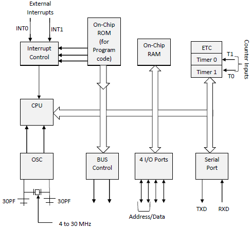
8051 microcontroller is designed by Intel in 1981. It is an 8-bit microcontroller. It is built with 40 pins DIP (dual inline package), 4kb of ROM storage and 128 bytes of RAM storage, 2 16-bit timers. It consists of are four parallel 8-bit ports, which are programmable as well as addressable as per the requirement. An on-chip crystal oscillator is integrated in the microcontroller having crystal frequency of 12 MHz.Let us now discuss the architecture of 8051 Microcontroller.
In the following diagram, the system bus connects all the support devices to the CPU. The system bus consists of an 8-bit data bus, a 16-bit address bus and bus control signals. All other devices like program memory, ports, data memory, serial interface, interrupt control, timers, and the CPU are all interfaced together through the system bus.

Data types and directives
The 8051 microcontroller is a popular microcontroller architecture that was originally developed by Intel. It has since become widely used and is produced by various manufacturers. The 8051 microcontroller has a versatile architecture with a variety of data types and directives. Here are some of the key aspects:
Data Types:
-
Bit: The smallest unit of data, representing a single binary digit (0 or 1).
-
Byte: A group of 8 bits, the fundamental unit for most data operations in the 8051.
-
Data (Internal) RAM: The 8051 has internal RAM (Random Access Memory) for data storage. The size of the RAM varies depending on the specific model of the 8051 microcontroller.
-
Register Banks: The 8051 has four register banks, each containing register locations that can be used for various purposes. The register banks are named R0 to R7.
-
Bit-Addressable RAM: Specific bits in the internal RAM can be individually addressed, allowing for efficient bit manipulation.
Directives:
-
ORG (Origin): Specifies the starting address for the code or data in memory.
-
DB (Define Byte): Allocates space in memory to store one or more bytes of data.
-
DW (Define Word): Allocates space in memory to store one or more 16-bit words.
-
DS (Define Storage): Reserves a block of memory for a specified number of bytes.
-
END: Marks the end of the assembly program.
-
EQU (Equate): Defines a constant or assigns a value to a symbol.
-
CODE: Specifies the segment of the program where the code is located.
-
DATA: Specifies the segment of the program where data is located.
-
SEGMENT: Declares a code or data segment.
-
ENDS: Marks the end of a segment.
PSW Register in 8051 Microcontroller | Program Status Word
2 Comments / By EFY / 21/05/2023
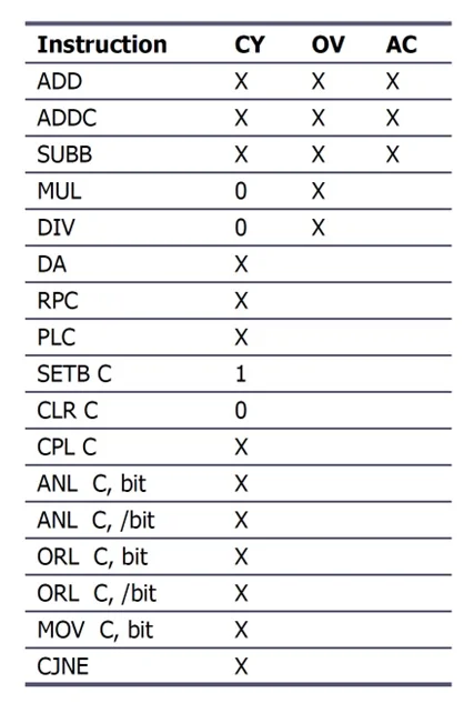
- Flags are single bit register and used to store the result of certain function after executing instruction. Flags are grouped inside PSW and PCON registers.
- PSW register in 8051 microcontroller contains math flags and PCON contains general user flags.
- Math flags are grouped in PSW of microcontroller 8051 and they are Carry(C), Auxiliary Carry (AC), Over flow (OV), and Parity (P). The general user flags are GF0 and GF1 which are grouped in PCON register.
PSW Register in 8051
- The PSW is accessible fully as an 8-bit register, with the address D0H.
- The bit pattern of this flag register is

Figure 1: Format of PSW register in 8051 Microcontroller
Parity Bit (P)
-
- This parity flag bit is used to show the number of 1s in the accumulator only. If the accumulator register contains an odd number of 1s, then this flag set to 1.
- If accumulator contains even number of 1s, then this flag cleared to 0.
Overflow Flag (OV)
-
- This flag is set during ALU operations, to indicate overflow in the result. It is set to 1 if there is a carry out of either the D7 bit or the D6 bit of the accumulator.
- Overflow flag is set when arithmetic operations such as add and subtract result in sign conflict.
-
- The conditions under which the OV flag is set are as follows: - Positive + Positive = Negative - Negative + Negative = Positive - Positive – Negative = Negative - Negative – Positive = Positive
Register Bank Select Bits (RS1 And RS0)
-
- These two bits are used to select one of four register banks of RAM. By setting and clearing these bits, registers R0-R7 are stored in one of four banks of RAM as follows.
| RS1 | RS0 | Bank Selected | Address of Registers |
|---|---|---|---|
| 0 | 0 | Bank 0 | 00h-07h |
| 0 | 1 | Bank 1 | 08h-0Fh |
| 1 | 0 | Bank 2 | 10h-17h |
| 1 | 1 | Bank 3 | 18h-1Fh |
| - - These bits are user-programmable. They can be set by the programmer to point to the correct register banks. | |||
| - The register bank selection in the programs can be changed using these two bits. |
General-Purpose Flag (F0)
-
- This is a user-programmable flag; the user can program and store any bit of his/her choice in this flag, using the bit address.
Auxiliary Carry Flag (AC)
-
- It is used in association with BCD arithmetic. This flag is set when there is a carry out of the D3 bit of the accumulator.
Carry Flag (CY)
-
- This flag is used to indicate the carry generated after arithmetic operations. It can also be used as an accumulator, to store one of the data bits for bit-related Boolean instructions.
-
The 8051 supports bit manipulation instructions.
- This means that in addition to the byte operations, bit operations can also be done using bit data.
- For this purpose, the contents of the PSW are bit-addressable.

8051 Register Bank and Stack
The 8051 microcontroller has a total of 128 bytes of RAM, organized into three groups:
- Register Bank and Stack (00H-1FH): 32 bytes
- Bit Addressable Read/Write Memory (20H-2FH): 16 bytes
- Scratch Pad - Read/Write Storage (30H-7FH): 80 bytes
Register Bank:
There are 4 register banks, each with 8 registers (R0 to R7), and each register is 8 bits wide. By default, Register Bank 0 is selected when the 8051 is powered up. The selection of other banks is done using bits D4 and D3 of the PSW (Program Status Word) register.
Stack:
The stack is a section of RAM used by the CPU to temporarily store information. The stack is accessed through the stack pointer (SP) register, which is 8 bits wide and can take values from 00 to FFH. Upon power-up, the SP register contains the value 07, indicating that RAM location 08 is the first location used for the stack. Storing data in the stack is referred to as a PUSH operation, and retrieving data from the stack into a CPU register is called a POP operation.
Example Code:
ORG 00H
MOV R1, #25H
MOV R4, #45H
PUSH 1
PUSH 4
POP 3
POP 6
END
- The instruction "PUSH 1" increments SP to 08H and pushes register R1 onto the stack location 08H.
- The "PUSH 4" instruction increments SP to 09H and pushes register R4 onto the stack location 09H.
- The instruction "POP 3" copies the top of the stack (location 09H) to register R3 and decrements SP to 08H.
- The "POP 6" instruction copies the top of the stack (location 08H) to register R6 and decrements SP to 07H.
Locations 08 to 1F can be used for the stack, with the upper limit of the stack being 1FH. If a program needs more than 24 bytes (08 to 1FH = 24 bytes) of stack, the SP can be changed to point to RAM locations 30 - 7FH using the instruction "MOV SP, #xxH". Initially, when the 8051 is powered up, SP is 07, and the first location of the stack is RAM location 08, which also belongs to register R0 of register bank 1. In other words, register bank 1 and the stack are using the same memory space.
If a program needs to use register banks 1 and 2, another section of RAM can be reallocated to the stack.
Reference
https://www.geeksforgeeks.org/microcontroller-and-its-types/ https://www.tutorialspoint.com/microprocessor/microcontrollers_8051_architecture.htm https://electronicsforyou.in/psw-register-in-8051-microcontroller/ https://www.refreshnotes.com/2016/03/8051-register-bank-and-stack.html