Question bank
1.Illustrate Microprocessor Technology.
Microprocessor technology refers to the design, development, and application of integrated circuits that contain the processing unit of a computer system. Here's an illustration of microprocessor technology:
1.Architecture: Microprocessors are built on a specific architecture, which defines the organization of its components and the set of instructions it can execute. Common architectures include x86, ARM, MIPS, and PowerPC, each with its own instruction set and design philosophy.
2.Components: A microprocessor typically consists of several key components: - Central Processing Unit (CPU): This is the core component responsible for executing instructions, performing arithmetic and logic operations, and controlling the flow of data within the system. - Registers: These are small, high-speed storage locations within the CPU used to store data temporarily during processing. - Control Unit (CU): This component manages the execution of instructions, fetching them from memory, decoding them, and controlling the operation of other components. - Arithmetic Logic Unit (ALU): The ALU performs arithmetic and logic operations on data, such as addition, subtraction, AND, OR, etc. - Cache Memory: This is a small, high-speed memory located close to the CPU that stores frequently accessed data and instructions to speed up processing. - Clock: Microprocessors operate synchronously with a clock signal, which regulates the timing of operations and ensures coordination between different components.
3.Instruction Set: Microprocessors understand and execute instructions encoded in machine language, which is represented as binary code. The instruction set architecture (ISA) defines the set of instructions that the microprocessor can execute, including arithmetic, logic, data transfer, and control instructions.
4.Memory Interface: Microprocessors interact with memory devices (RAM, ROM, etc.) to store and retrieve data and instructions. They use memory addresses to access specific locations in memory and transfer data between memory and the CPU.
5. Peripheral Interfaces**: Microprocessors communicate with external devices, such as input/output (I/O) devices, through various interfaces like serial ports, parallel ports, USB ports, Ethernet, etc. These interfaces allow the microprocessor to interact with the external world, enabling functions like data input, output, and communication.
6.Applications: Microprocessors are used in a wide range of applications, including personal computers, smartphones, embedded systems, automotive electronics, industrial control systems, and consumer electronics. Their versatility, high performance, and cost-effectiveness make them suitable for diverse computing tasks.
In summary, microprocessor technology encompasses the design, architecture, components, instruction set, memory interface, peripheral interfaces, and applications of microprocessors, which are essential components of modern computing systems.
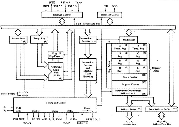
2.Draw the Architectural diagram of microprocessor 8085.
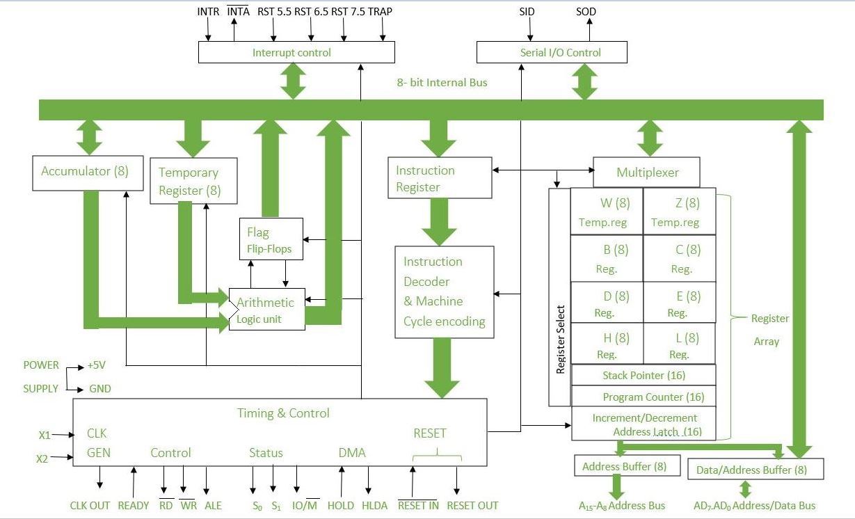
3.Explain the Architectural diagram of microprocessor 8085.
Microprocessor-8085 Architecture
8085 is pronounced as "eighty-eighty-five" microprocessor. It is an 8-bit microprocessor designed by Intel in 1977 using NMOS technology.
It has the following configuration −
- 8-bit data bus
- 16-bit address bus, which can address upto 64KB
- A 16-bit program counter
- A 16-bit stack pointer
- Six 8-bit registers arranged in pairs: BC, DE, HL
- Requires +5V supply to operate at 3.2 MHZ single phase clock
It is used in washing machines, microwave ovens, mobile phones, etc.
8085 Microprocessor – Functional Units
8085 consists of the following functional units −
Accumulator
It is an 8-bit register used to perform arithmetic, logical, I/O & LOAD/STORE operations. It is connected to internal data bus & ALU.
Arithmetic and logic unit
As the name suggests, it performs arithmetic and logical operations like Addition, Subtraction, AND, OR, etc. on 8-bit data.
General purpose register
There are 6 general purpose registers in 8085 processor, i.e. B, C, D, E, H & L. Each register can hold 8-bit data.
These registers can work in pair to hold 16-bit data and their pairing combination is like B-C, D-E & H-L.
Program counter
It is a 16-bit register used to store the memory address location of the next instruction to be executed. Microprocessor increments the program whenever an instruction is being executed, so that the program counter points to the memory address of the next instruction that is going to be executed.
Stack pointer
It is also a 16-bit register works like stack, which is always incremented/decremented by 2 during push & pop operations.
Temporary register
It is an 8-bit register, which holds the temporary data of arithmetic and logical operations.
Flag register
It is an 8-bit register having five 1-bit flip-flops, which holds either 0 or 1 depending upon the result stored in the accumulator.
These are the set of 5 flip-flops −
- Sign (S)
- Zero (Z)
- Auxiliary Carry (AC)
- Parity (P)
- Carry (C)
Its bit position is shown in the following table −
| D7 | D6 | D5 | D4 | D3 | D2 | D1 | D0 |
|---|---|---|---|---|---|---|---|
| S | Z | AC | P | CY | |||
| Instruction register and decoder |
It is an 8-bit register. When an instruction is fetched from memory then it is stored in the Instruction register. Instruction decoder decodes the information present in the Instruction register.
Timing and control unit
It provides timing and control signal to the microprocessor to perform operations. Following are the timing and control signals, which control external and internal circuits −
- Control Signals: READY, RD’, WR’, ALE
- Status Signals: S0, S1, IO/M’
- DMA Signals: HOLD, HLDA
- RESET Signals: RESET IN, RESET OUT
Interrupt control
As the name suggests it controls the interrupts during a process. When a microprocessor is executing a main program and whenever an interrupt occurs, the microprocessor shifts the control from the main program to process the incoming request. After the request is completed, the control goes back to the main program.
There are 5 interrupt signals in 8085 microprocessor: INTR, RST 7.5, RST 6.5, RST 5.5, TRAP.
Serial Input/output control
It controls the serial data communication by using these two instructions: SID (Serial input data) and SOD (Serial output data).
Address buffer and address-data buffer
The content stored in the stack pointer and program counter is loaded into the address buffer and address-data buffer to communicate with the CPU. The memory and I/O chips are connected to these buses; the CPU can exchange the desired data with the memory and I/O chips.
Address bus and data bus
Data bus carries the data to be stored. It is bidirectional, whereas address bus carries the location to where it should be stored and it is unidirectional. It is used to transfer the data & Address I/O devices.
4.Draw the Architectural diagram of microprocessor 8086.
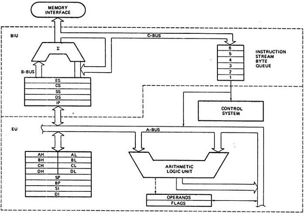
5.Explain the Architectural diagram of microprocessor 8086.
8086 Microprocessor is an enhanced version of 8085Microprocessor that was designed by Intel in 1976. It is a 16-bit Microprocessor having 20 address lines and16 data lines that provides up to 1MB storage. It consists of powerful instruction set, which provides operations like multiplication and division easily.
It supports two modes of operation, i.e. Maximum mode and Minimum mode. Maximum mode is suitable for system having multiple processors and Minimum mode is suitable for system having a single processor.
Features of 8086
The most prominent features of a 8086 microprocessor are as follows −
-
It has an instruction queue, which is capable of storing six instruction bytes from the memory resulting in faster processing.
-
It was the first 16-bit processor having 16-bit ALU, 16-bit registers, internal data bus, and 16-bit external data bus resulting in faster processing.
-
It is available in 3 versions based on the frequency of operation −
-
8086 → 5MHz
-
8086-2 → 8MHz
-
(c)8086-1 → 10 MHz
-
-
It uses two stages of pipelining, i.e. Fetch Stage and Execute Stage, which improves performance.
-
Fetch stage can prefetch up to 6 bytes of instructions and stores them in the queue.
-
Execute stage executes these instructions.
-
It has 256 vectored interrupts.
-
It consists of 29,000 transistors.
Architecture of 8086
The following diagram depicts the architecture of a 8086 Microprocessor −
6.What are the different features of 8085 designer must considered to develop the 8085 based system?
To develop an 8085-based system effectively, designers must consider various features and specifications of the Intel 8085 microprocessor. Here are the key features that designers should take into account:
-
Architecture: Understand the architecture of the 8085 microprocessor, including its organization of registers, data bus, address bus, control signals, and instruction set architecture (ISA). This knowledge is essential for designing the overall system and interfacing with peripheral devices.
-
Clock Frequency: Determine the operating frequency of the 8085 microprocessor, which affects the overall performance of the system. Design the system to provide a stable clock signal within the specified frequency range to ensure proper synchronization of operations.
-
Power Supply Requirements: Consider the power supply specifications of the 8085 microprocessor, including voltage levels, current requirements, and power consumption. Design the power supply circuitry to meet these requirements and ensure reliable operation of the system.
-
Memory Interface: Understand the memory addressing capabilities of the 8085 microprocessor, including its support for various types of memory devices such as RAM, ROM, and I/O ports. Design the memory interface circuitry to accommodate the memory requirements of the system and facilitate efficient data transfer.
-
Input/Output Interface: Take into account the input/output (I/O) capabilities of the 8085 microprocessor, including its support for interfacing with external devices such as keyboards, displays, sensors, and actuators. Design the I/O interface circuitry to enable communication between the microprocessor and external peripherals.
-
Interrupt Handling: Understand the interrupt handling mechanism of the 8085 microprocessor, including its support for different types of interrupts and interrupt priority levels. Design the system to handle interrupts effectively and ensure timely response to interrupt requests from external devices.
-
Address Decoding: Implement proper address decoding logic to enable the microprocessor to access different memory and I/O devices within the system. Design the address decoding circuitry to generate chip select signals for the selected memory or I/O device based on the address lines provided by the microprocessor.
-
Peripheral Interfacing: Ensure compatibility with standard peripheral interface protocols such as RS-232, SPI, I2C, etc., to facilitate communication with external devices. Design the interface circuitry to support the required communication protocol and data transfer rates.
-
System Integration and Testing: Integrate the 8085 microprocessor into the overall system design and conduct thorough testing to verify proper functionality and performance. Test the system with different input scenarios and verify the output to ensure that it meets the desired specifications.
By considering these features and specifications of the 8085 microprocessor, designers can develop efficient and reliable systems tailored to specific application requirements.
7.Explain the Flag Register of 8085 Microprocessor.
Flag register in 8085 microprocessor
The Flag register is a Special Purpose Register. Depending upon the value of the result after any arithmetic and logical operation, the flag bits become set (1) or reset (0). In 8085 microprocessor, the flag register consists of 8 bits and only 5 of them are useful. The 5 flags are:
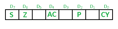
1.Sign Flag (S) – After any operation if the MSB (B(7)) of the result is 1, it indicates the number is negative and the sign flag becomes set, i.e. 1. If the MSB is 0, it indicates the number is positive and the sign flag becomes reset i.e. 0. from 00H to 7F, sign flag is 0 from 80H to FF, sign flag is 1 1- MSB is 1 (negative) 0- MSB is 0 (positive)
Example: MVI A 30 (load 30H in register A) MVI B 40 (load 40H in register B) SUB B (A = A – B) These set of instructions will set the sign flag to 1 as 30 – 40 is a negative number. MVI A 40 (load 40H in register A) MVI B 30 (load 30H in register B) SUB B (A = A – B) These set of instructions will reset the sign flag to 0 as 40 – 30 is a positive number.
2.Zero Flag (Z) – After any arithmetical or logical operation if the result is 0 (00)H, the zero flag becomes set i.e. 1, otherwise it becomes reset i.e. 0. 00H zero flags is 1. from 01H to FFH zero flag is 0 1- zero-result 0- non-zero result
Example: MVI A 10 (load 10H in register A) SUB A (A = A – A) These set of instructions will set the zero flag to 1 as 10H – 10H is 00H
3.Auxiliary Carry Flag (AC) – This flag is used in the BCD number system(0-9). If after any arithmetic or logical operation D(3) generates any carry and passes it on to D(4) this flag becomes set i.e. 1, otherwise, it becomes reset i.e. 0. This is the only flag register that is not accessible by the programmer 1-carry out from bit 3 on addition or borrows into bit 3 on subtraction 0-otherwise
Example: MVI A 2BH (load 2BH in register A) MVI 39H (load 39H in register B) ADD B (A = A + B) These set of instructions will set the auxiliary carry flag to 1, as on adding 2B and 39, the addition of lower-order nibbles B and 9 will generate a carry.
4.Parity Flag (P) – If after any arithmetic or logical operation the result has even parity, an even number of 1 bit, the parity register becomes set i.e. 1, otherwise it becomes reset i.e. 0. 1-accumulator has an even number of 1 bits 0-accumulator has odd parity
Example: MVI A 05 (load 05H in register A) This instruction will set the parity flag to 1 as the BCD code of 05H is 00000101, which contains an even number of ones i.e. 2.
5.Carry Flag (CY) – Carry is generated when performing n bit operations and the result is more than n bits, then this flag becomes set i.e. 1, otherwise, it becomes reset i.e. 0. During subtraction (A-B), if A>B it becomes reset, and if (A<B) it becomes set. Carry flag is also called the borrow flag. 1-carry out from MSB bit on addition or borrow into MSB bit on subtraction 0-no carry out or borrow into MSB bit.
Example: MVI A 30 (load 30H in register A) MVI B 40 (load 40H in register B) SUB B (A = A – B) These set of instructions will set the carry flag to 1 as 30 – 40 generates a carry/borrow. MVI A 40 (load 40H in register A) MVI B 30 (load 30H in register B) SUB B (A = A – B) These set of instructions will reset the carry flag to 0 as 40 – 30 does not generate any carry/borrow.
8.What are the different features of 8086 designer must considered to develop the 8085 based system?
- Architecture: Understand the differences in architecture between the 8086 and 8085 processors, including the register set, instruction set, and memory addressing modes.
- Compatibility Mode: The 8086 can operate in a backward-compatible mode (real mode) to execute 8085 instructions. Designers should consider this mode for compatibility with existing software.
- Memory Segmentation: The 8086 uses memory segmentation, unlike the 8085. Designers must account for this and handle memory addressing accordingly.
- Interrupt Handling: The interrupt handling mechanism in the 8086 differs from that of the 8085. Designers should ensure compatibility or adapt interrupt handling routines accordingly.
- Data and Address Bus: The 8086 has a 16-bit data bus and a 20-bit address bus, whereas the 8085 has an 8-bit data bus and a 16-bit address bus. Designers need to interface the 8086 appropriately to accommodate these differences.
9.Explain the Flag Register of 8086 Microprocessor.
The flag register, also known as the FLAGS register, is a crucial component of the Intel 8086 microprocessor architecture. It contains a set of status flags that reflect the outcomes of arithmetic and logic operations performed by the CPU. Understanding the flag register is essential for writing efficient assembly language programs and for implementing conditional branching and decision-making logic. Here's an explanation of the flag register of the 8086 microprocessor:
1. Bit Structure: The flag register is a 16-bit register, with each bit representing a specific flag. The flags are numbered from 0 to 15, with some flags having specific meanings and others being reserved for future use.
2. Common Flags:
- Carry Flag (CF): This flag indicates whether a carry occurred during arithmetic operations like addition or subtraction. It is also used in multi-precision arithmetic and logical shift operations.
- Zero Flag (ZF): This flag is set when the result of an operation is zero. It is cleared when the result is non-zero.
- Sign Flag (SF): This flag reflects the sign of the result. It is set if the result is negative (has the most significant bit set) and cleared otherwise.
- Overflow Flag (OF): This flag indicates whether an overflow occurred during signed arithmetic operations. An overflow occurs when the result cannot be represented within the available number of bits.
- Auxiliary Carry Flag (AF): This flag is used for binary-coded decimal (BCD) arithmetic operations. It indicates whether a carry occurred from the low nibble (bits 0-3) to the high nibble (bits 4-7) during addition or subtraction.
- Parity Flag (PF): This flag indicates the parity of the least significant byte of the result. It is set if the number of set bits in the least significant byte is even and cleared if it is odd.
3. Conditional Branching: The flags in the flag register are used to implement conditional branching instructions such as JUMP IF ZERO (JZ), JUMP IF NOT ZERO (JNZ), JUMP IF CARRY (JC), etc. These instructions allow the CPU to change the flow of program execution based on the current state of the flags.
4. Status Reporting: In addition to influencing program flow, the flags in the flag register can also be examined by the program to make decisions or perform specific actions based on the results of previous operations.
5. Flag Manipulation: Assembly language instructions exist to manipulate the flags directly, such as the CLC (clear carry flag), STC (set carry flag), and CMC (complement carry flag) instructions. These instructions are useful for controlling program flow or preparing the CPU for subsequent operations.
In summary, the flag register of the 8086 microprocessor is a critical component that reflects the outcomes of arithmetic and logic operations, influences program flow through conditional branching, and can be directly manipulated by assembly language instructions. Understanding the flag register is essential for effective programming and utilization of the 8086 microprocessor.
10.Explain the functionality of each Pin of 8085 Microprocessor with neat diagram?
The following image depicts the pin diagram of 8085 Microprocessor −
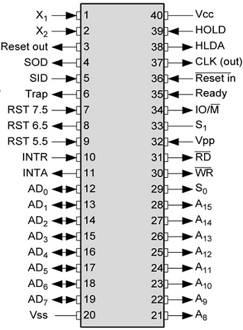
The pins of a 8085 microprocessor can be classified into seven groups −
Address bus
A15-A8, it carries the most significant 8-bits of memory/IO address.
Data bus
AD7-AD0, it carries the least significant 8-bit address and data bus.
Control and status signals
These signals are used to identify the nature of operation. There are 3 control signal and 3 status signals.
Three control signals are RD, WR & ALE.
-
RD − This signal indicates that the selected IO or memory device is to be read and is ready for accepting data available on the data bus.
-
WR − This signal indicates that the data on the data bus is to be written into a selected memory or IO location.
-
ALE − It is a positive going pulse generated when a new operation is started by the microprocessor. When the pulse goes high, it indicates address. When the pulse goes down it indicates data.
Three status signals are IO/M, S0 & S1.
IO/M
This signal is used to differentiate between IO and Memory operations, i.e. when it is high indicates IO operation and when it is low then it indicates memory operation.
S1 & S0
These signals are used to identify the type of current operation.
Power supply
There are 2 power supply signals − VCC & VSS. VCC indicates +5v power supply and VSS indicates ground signal.
Clock signals
There are 3 clock signals, i.e. X1, X2, CLK OUT.
-
X1, X2 − A crystal (RC, LC N/W) is connected at these two pins and is used to set frequency of the internal clock generator. This frequency is internally divided by 2.
-
CLK OUT − This signal is used as the system clock for devices connected with the microprocessor.
Interrupts & externally initiated signals
Interrupts are the signals generated by external devices to request the microprocessor to perform a task. There are 5 interrupt signals, i.e. TRAP, RST 7.5, RST 6.5, RST 5.5, and INTR. We will discuss interrupts in detail in interrupts section.
-
INTA − It is an interrupt acknowledgment signal.
-
RESET IN − This signal is used to reset the microprocessor by setting the program counter to zero.
-
RESET OUT − This signal is used to reset all the connected devices when the microprocessor is reset.
-
READY − This signal indicates that the device is ready to send or receive data. If READY is low, then the CPU has to wait for READY to go high.
-
HOLD − This signal indicates that another master is requesting the use of the address and data buses.
-
HLDA (HOLD Acknowledge) − It indicates that the CPU has received the HOLD request and it will relinquish the bus in the next clock cycle. HLDA is set to low after the HOLD signal is removed.
Serial I/O signals
There are 2 serial signals, i.e. SID and SOD and these signals are used for serial communication.
-
SOD (Serial output data line) − The output SOD is set/reset as specified by the SIM instruction.
-
SID (Serial input data line) − The data on this line is loaded into accumulator whenever a RIM instruction is executed.
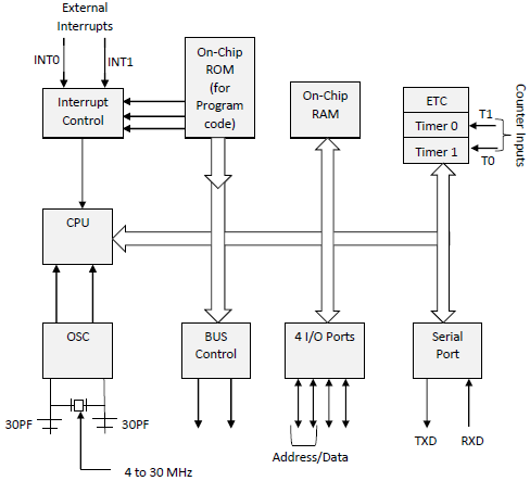
11.Compare Microcontroller and Microprocessor.
| Parameter | Microprocessor | Microcontroller |
|---|---|---|
| Definition | Heart of a computer system | Heart of an embedded system |
| What is it? | Processor with memory and I/O connected externally | Controlling device with internal memory and I/O components |
| Circuit complexity | Complex due to external connections | Less complex due to on-chip memory |
| Memory and I/O components | Connected externally | Internal memory and I/O components available |
| Compact system compatibility | Can't be used in compact systems | Compatible with compact systems |
| Efficiency | Less efficient | More efficient |
| Zero status flag | Has a zero status flag | Doesn't have a zero status flag |
| Number of registers | Less number of registers | More number of registers |
| Applications | Generally used in personal computers | Commonly used in appliances like washing machines, air conditioners |
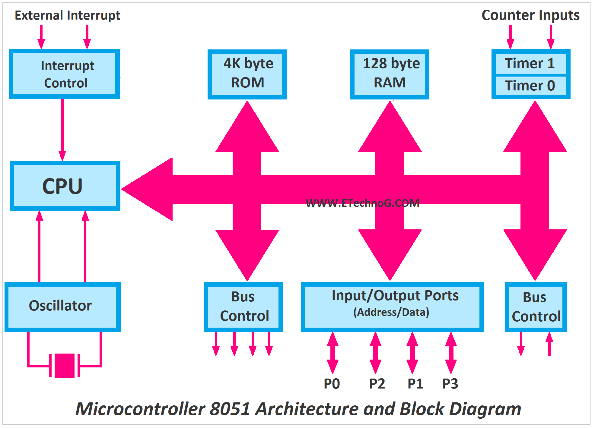
12.Draw the Architectural diagram of 8051 microcontrollers.
13.Explain the Architectural diagram of 8051 microcontrollers.
8051 Microcontroller Architecture
Let's see the internal architecture of 8051 Microcontroller represented in form of block diagram as shown below:
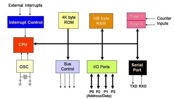
Basic components present internally inside 8051 Microcontroller architecture are:
CPU (Central Processing Unit): CPU act as a mind of any processing machine. It synchronizes and manages all processes that are carried out in microcontroller. User has no power to control the functioning of CPU. It interprets the program stored in ROM and carries out from storage and then performs it projected duty. CPU manage the different types of registers available in 8051 microcontroller.
Interrupts: Interrupts is a sub-routine call that given by the microcontroller when some other program with high priority is request for acquiring the system buses the n interrupts occur in current running program.
Interrupts provide a method to postpone or delay the current process, performs a sub-routine task and then restart the standard program again.
Types of interrupt in 8051 Microcontroller:
Let's see the five sources of interrupts in 8051 Microcontroller:
- Timer 0 overflow interrupt - TF0
- Timer 1 overflow interrupt - TF1
- External hardware interrupt - INT0
- External hardware interrupt - INT1
- Serial communication interrupt - RI/TI
Memory: For operation Micro-controller required a program. This program guides the microcontroller to perform the specific tasks. This program installed in microcontroller required some on chip memory for the storage of the program.
Microcontroller also required memory for storage of data and operands for the short duration. In microcontroller 8051 there is code or program memory of 4 KB that is it has 4 KB ROM and it also comprise of data memory (RAM) of 128 bytes.
Bus : Bus is a group of wires which uses as a communication canal or acts as means of data transfer. The different bus configuration includes 8, 16 or more cables. Therefore, a bus can bear 8 bits, 16 bits all together.
Types of buses in 8051 Microcontroller:
Let's see the two types of bus used in 8051 microcontroller:
- Address Bus: 8051 microcontrollers is consisting of 16 bit address bus. It is generally be used for transferring the data from Central Processing Unit to Memory.
- Data bus: 8051 microcontroller is consisting of 8 bits data bus. It is generally be used for transferring the data from one peripherals position to other peripherals.
Oscillator: As the microcontroller is digital circuit therefore it needs timer for their operation. To perform timer operation inside microcontroller it required externally connected or on-chip oscillator. Microcontroller is used inside an embedded system for managing the function of devices. Therefore, 8051 uses the two 16 bit counters and timers. For the operation of this timers and counters the oscillator is used inside microcontroller.
14.Illustrate data types and directives of 8051 microcontroller.
In the 8051 microcontroller architecture, data types and directives play crucial roles in defining data elements, organizing memory, and guiding the assembler during the compilation process. Let's illustrate the commonly used data types and directives in the context of programming the 8051 microcontroller:
Data Types in 8051 Microcontroller:
-
Byte (8-bit): This is the most basic data type in the 8051 microcontroller. It occupies one byte (8 bits) of memory and can represent values from 0 to 255 (unsigned) or -128 to 127 (signed).
-
Word (16-bit): A word consists of two bytes (16 bits) of memory. It can represent larger values than a byte, ranging from 0 to 65535 (unsigned) or -32768 to 32767 (signed).
-
Bit: The 8051 microcontroller provides support for bit-level operations. Individual bits within memory locations can be manipulated using bitwise operators. Bit variables are often used for flags, status indicators, or control signals.
-
Data Pointer (DPTR): The Data Pointer is a 16-bit register used for accessing external memory locations. It is commonly used for indirect addressing and accessing data stored in external memory devices.
-
Special Function Registers (SFRs): These are memory-mapped registers within the 8051 microcontroller that control various on-chip peripherals and functions. SFRs have specific addresses and bit-level access for configuring and controlling the microcontroller's behavior.
Directives in 8051 Microcontroller:
-
ORG (Origin): This directive specifies the starting address of the code or data in memory. It is used to define the memory location where the subsequent code or data will be stored.
-
DB (Define Byte): DB directive is used to define byte-sized data elements in memory. It allows programmers to assign initial values to memory locations or reserve memory space for variables.
-
DW (Define Word): DW directive is similar to DB but is used to define word-sized (16-bit) data elements in memory. It is commonly used for storing larger numerical values or data structures.
-
DS (Define Storage): DS directive is used to reserve memory space without initializing it. It specifies the number of bytes to allocate in memory for variables or data structures.
-
END: The END directive marks the end of the assembly source file. It informs the assembler that it has reached the end of the program and stops the assembly process.
-
INCLUDE: The INCLUDE directive is used to include the contents of another file into the current assembly source file. It is helpful for modularizing code and reusing common routines or data definitions.
By utilizing these data types and directives effectively, programmers can write efficient and well-organized assembly language programs for the 8051 microcontroller, ensuring optimal utilization of resources and ease of maintenance.
15.Explain the PSW Register of 8051 Microcontroller.
PSW Register in 8051 Microcontroller | Program Status Word
- Flags are single bit register and used to store the result of certain function after executing instruction. Flags are grouped inside PSW and PCON registers.
- PSW register in 8051 microcontroller contains math flags and PCON contains general user flags.
- Math flags are grouped in PSW of microcontroller 8051 and they are Carry(C), Auxiliary Carry (AC), Over flow (OV), and Parity (P). The general user flags are GF0 and GF1 which are grouped in PCON register.
PSW Register in 8051
- The PSW is accessible fully as an 8-bit register, with the address D0H.
- The bit pattern of this flag register is

Figure 1: Format of PSW register in 8051 Microcontroller
Parity Bit (P)
-
- This parity flag bit is used to show the number of 1s in the accumulator only. If the accumulator register contains an odd number of 1s, then this flag set to 1.
- If accumulator contains even number of 1s, then this flag cleared to 0.
Overflow Flag (OV)
-
- This flag is set during ALU operations, to indicate overflow in the result. It is set to 1 if there is a carry out of either the D7 bit or the D6 bit of the accumulator.
- Overflow flag is set when arithmetic operations such as add and subtract result in sign conflict.
-
- The conditions under which the OV flag is set are as follows: - Positive + Positive = Negative - Negative + Negative = Positive - Positive – Negative = Negative - Negative – Positive = Positive
Register Bank Select Bits (RS1 And RS0)
-
- These two bits are used to select one of four register banks of RAM. By setting and clearing these bits, registers R0-R7 are stored in one of four banks of RAM as follows.
| RS1 | RS0 | Bank Selected | Address of Registers |
|---|---|---|---|
| 0 | 0 | Bank 0 | 00h-07h |
| 0 | 1 | Bank 1 | 08h-0Fh |
| 1 | 0 | Bank 2 | 10h-17h |
| 1 | 1 | Bank 3 | 18h-1Fh |
-
- These bits are user-programmable. They can be set by the programmer to point to the correct register banks.
- The register bank selection in the programs can be changed using these two bits.
General-Purpose Flag (F0)
-
- This is a user-programmable flag; the user can program and store any bit of his/her choice in this flag, using the bit address.
Auxiliary Carry Flag (AC)
-
- It is used in association with BCD arithmetic. This flag is set when there is a carry out of the D3 bit of the accumulator.
Carry Flag (CY)
-
- This flag is used to indicate the carry generated after arithmetic operations. It can also be used as an accumulator, to store one of the data bits for bit-related Boolean instructions.
-
The 8051 supports bit manipulation instructions.
- This means that in addition to the byte operations, bit operations can also be done using bit data.
- For this purpose, the contents of the PSW are bit-addressable.

Figure 2: Instructions that affect the flags in 8051 microcontroller
16.List the features of 8051 Microcontroller.
- CPU Core: 8-bit microcontroller with a Harvard architecture.
- Memory: Typically includes on-chip ROM, RAM, and EEPROM.
- I/O Ports: Multiple I/O ports for interfacing with external devices.
- Timers/Counters: Integrated timers/counters for time-sensitive applications.
- Serial Communication: UART for serial communication.
- Interrupt System: Supports external and internal interrupts.
- Clock Circuitry: Built-in oscillator or support for external clock sources.
17.Discuss the programming model of microcontroller 8051.
The programming model of the 8051 microcontroller provides a framework for understanding how instructions are executed, how data is accessed, and how the various components of the microcontroller interact. The programming model of the 8051 consists of several key elements, including registers, memory, and I/O ports. Let's discuss each component in detail:
1. Registers:
- Accumulator (ACC): The accumulator is an 8-bit register used for arithmetic and logic operations. It holds one of the operands during these operations and stores the result.
- B Register: Similar to the accumulator, the B register is an 8-bit register used for arithmetic and logic operations. It can be used as a second accumulator or as a general-purpose register.
- Data Pointer (DPTR): The Data Pointer is a 16-bit register used for accessing external memory locations. It is commonly used for indirect addressing and accessing data stored in external memory devices.
- Program Counter (PC): The program counter is a 16-bit register that holds the address of the next instruction to be executed. It is automatically incremented after each instruction fetch.
- Stack Pointer (SP): The stack pointer is an 8-bit register that points to the top of the stack. It is used to manage subroutine calls and interrupt handling.
- Status Register (PSW): The status register, also known as the Program Status Word, is an 8-bit register that contains various flags indicating the outcomes of arithmetic and logic operations, as well as the status of the microcontroller.
- Timer/Counter Registers (TMRx, THx, TLx): The 8051 microcontroller has one or more timer/counter registers used for timing and counting operations. These registers are used to generate timing delays, measure time intervals, and interface with external devices.
2. Memory:
- Internal RAM: The 8051 microcontroller typically contains on-chip random-access memory (RAM) used for storing data and variables during program execution. The size of the internal RAM varies depending on the specific model of the 8051.
- Internal ROM: Some variants of the 8051 microcontroller include on-chip read-only memory (ROM) used for storing the program code. The size of the internal ROM varies, and it typically contains the bootloader or firmware code.
- External RAM/ROM: The 8051 microcontroller can also interface with external memory devices such as RAM and ROM chips. The Data Pointer (DPTR) register is used for accessing external memory locations.
3. I/O Ports:
- The 8051 microcontroller features multiple input/output (I/O) ports used for interfacing with external devices such as sensors, actuators, displays, and communication modules.
- Each I/O port typically consists of 8 bits and can be configured as input or output using software instructions.
- Special Function Registers (SFRs) are used to control and configure the behavior of the I/O ports.
In summary, the programming model of the 8051 microcontroller encompasses registers, memory, and I/O ports, which are essential for writing assembly language programs and controlling the behavior of the microcontroller. Understanding the programming model helps programmers effectively utilize the resources of the 8051 microcontroller and develop efficient embedded systems applications.
18.Explain the Stack of microcontroller 8051.
Stack of Microcontroller 8051:
- The 8051 microcontroller uses a stack to store return addresses, register values, and other data during subroutine calls and interrupt handling.
- It typically consists of a stack pointer (SP) register, which points to the top of the stack.
- The stack grows downwards in memory, meaning that as items are pushed onto the stack, the stack pointer decrements.
- The stack is used to store the return address when a subroutine is called, allowing the program to return to the correct location after the subroutine finishes execution.
- Additionally, the stack is used to save the context (register values) when an interrupt occurs, ensuring that the main program can resume execution after handling the interrupt.
19.Illustrate the concept of register bank of microcontroller 8051.
Register Bank of Microcontroller 8051:
- The 8051 microcontroller features four register banks, labeled as bank 0, bank 1, bank 2, and bank 3.
- Each register bank contains the same set of registers: R0 to R7 (eight general-purpose registers) and a few special function registers (SFRs).
- The register banks are used to provide more register space for data storage and manipulation, especially in applications with a large number of variables or complex calculations.
- The 8051's architecture allows the programmer to switch between register banks using certain instructions, enabling efficient use of the available registers and facilitating context switching in multitasking applications.
20.List the data type of 8051? Describe the functions of assembler directives of 8051.
Data Types of 8051 and Functions of Assembler Directives:
-
Data Types: The 8051 supports various data types, including:
- 8-bit unsigned integers (unsigned char).
- 16-bit unsigned integers (unsigned int).
- 8-bit signed integers (signed char).
- 16-bit signed integers (signed int).
- Bit (Boolean) data type.
-
Assembler Directives: Assembler directives in 8051 assembly language provide instructions to the assembler rather than the CPU. They include:
- ORG: Specifies the origin address for the subsequent code or data.
- DB (Define Byte): Defines byte-sized data.
- DW (Define Word): Defines word-sized data.
- DS (Define Storage): Reserves memory space without initializing it.
- END: Marks the end of the assembly file.
- INCLUDE: Includes contents of another file in the current assembly file.